Semiconductor
Backed Strain Gages
Introduction
Piezo-Metrics offers a line of Semiconductor - Backed Gages.
- Easy to Install Mounted on a flexible insulated circuit with versatile solder pads makes this device easy to install. The gage and gold wires are over-coated to seal out moisture and to provide additional protection of the gage during the application process.
-
Flexible
Flexible enough to bend around a 0.5 inch diameter rod.
- Performance Sensitivity is 50 to 75 times greater than a foil gage.
- Linearity & Stability On load cells and foil bridges our gages can be used as a linearity corrector. A non-linearity of 0.125 % FS can be corrected to less than .05 % of full scale. Long-term stability is not compromised.
- Suggested Uses Prototyping for proof of concept and for transient or high frequency measurements.
 |
 |
|
|
 |
Backed Semiconductor Strain Gages
Part Number |
Width |
Lead Attachment |
Thickness |
Resistance Ohms@ 78° |
Gage Factor |
TCGF |
TCR |
|---|---|---|---|---|---|---|---|
| SS-027-013-500PB | .009 | Ball Bond | .0004 | 540±50 | 155±10 | -18% | 24% |
| SS-037-022-500PB | .009 | Ball Bond | .0004 | 540±50 | 155±10 | -13% | 17% |
| SS-060-033-500PB | .008 | WL | .0004 | 540±50 | 140±10 | -13% | 15% |
| SS-060-033-500PUB | .016 | WL | .0004 | 540±50 | 140±10 | -12% | 14% |
| SS-060-033-1000PB | .008 | WL | .0004 | 1050±75 | 155±10 | -18% | 24% |
| SS-060-033-2000PUB | .016 | WL | .0004 | 2000±1000 | 155±100 | -18% | 25% |
| SS-060-033-5000PB | .008 | WL | .0004 | 5000±500 | 175±500 | -23% | 47% |
| SS-080-050-120PB | .008 | WL | .0004 | 120±20 | 120±10 | -9% | 5% |
| SS-080-050-230PB | .008 | WL | .0004 | 230±30 | 120±10 | -9% | 5% |
| SS-080-050-345PB | .008 | WL | .0004 | 345±40 | 140±10 | -13% | 16% |
| SS-080-050-500PB | .008 | WL | .0004 | 540±50 | 140±50 | -13% | 16% |
| SS-080-050-10,000PUB | .008 | WL | .0004 | 10000±1000 | 175±10 | -23% | 42% |
| SS-095-060-350PUB | .016 | WL | .0004 | 350±50 | 120±10 | -9% | 5% |
| SS-090-060-1150PB | .008 | WL | .0004 | 1125±75 | 155±10 | -18% | 24% |
| SS-150-124-15PB | .009 | WL | .0010 | 15±2 | 100±10 | -10% | 6% |
| SS-150-124-25PB | .008 | WL | .0008 | 25±3 | 100±10 | -10% | 6% |
| SS-150-124-30PB | .008 | WL | .0008 | 30±4 | 100±10 | -10% | 6% |
| SS-150-124-40PB | .008 | WL | .0008 | 40±4 | 100±10 | -10% | 6% |
| SS-250-225-120PB | .009 | WL | .0004 | 120±20 | 100±10 | -10% | 6% |
Ordering Guidelines and Examples
B > C > D > E > F > G > H |
SS > 080 >050 > 120 > P > > B >S2 |
||||
|---|---|---|---|---|---|
| A. Model (SS) | SS-080-050-500P U S4 is a Semiconductor Strain gage with a total length of 080 and an active length of 050. The gage has a nominal resistance of 500 at 78 degrees F. The gage is further defined as Dopant P and Configured as a “U”* Gage. S4 specifies a matched set of 4 gages. |
B. Total Length | |||
| C. Active Length |
| ||||
| D. Nominal Resistance at 78° F | |||||
| E. Dopant | |||||
| F. U Gage, M Gage, or Leave Blank for Bar Gage* | |||||
| G. B Specifies backed gages | |||||
| H. Specifies Single or Matched Gages |
Standard Bridge Matching
| Temperature°F Standard Matching |
0°F ±0.6% |
78°F ±0.4% |
278°F ±0.4% |
Percent of Base Resistance |
Note: Custom special matching gages (Mil-Spec.) or additional data points are also available.
Please contact Piezo-Metrics for details. Phone: (805) 522-4676
Semiconductor Strain Gages have large temperature coefficients of resistance making single gage strain measurements difficult unless used at a constant temperature. For this reason, gages are predominantly used in a half bridge or full bridge circuits and carefully matched for slope and intercept.
Part Number Details
- SS-060-033-500P-S2
SS designated Semiconductor Strain Gage.
060 designated the gage is 0.060 long.
033 designates the gage has an active area in the center of 0.033.
500P designates 500 ohms nominally at room temperature and it is P-doped.
S2 indicates these two gages are resistance versus temperature matched to each other.
Standard Packaging
Gages are packed in clear plastic boxes measuring approximately one inch square.
Each clear box lid is labeled with information about the gage.

- Temperature °F is noted along with the corresponding Resistance in Ω
| Ohms | 0°F | 477 |
| 78°F | 517 |
| 278°F | 674 |
- Gage lot Number is marked as Lt.
- Computer System number used to measure the resistance over temperature
- Gage Position Number identifies the position of the gage on the board in the temperature chamber.
Notes:
- The computer system also measures and records reverse current and TCR ( Thermal Coefficient of Resistance ). This data is used to detect nonperforming gages allowing them to be removed from production.
- Gages are package one gage to a clear box with each box having its own
label. Matched sets will be joined together with clear plastic tape on the
bottom of the boxes.

Matched Gage Information
There are many uses for semiconductor strain gages and to accommodate these applications, Piezo-Metrics offers a number of matching options. SS-060-033-500P-xx
S1 is a single gage, tested and with data.
S2 is a thermally matched set of two gages, tested with data. S4 is a thermally matched set of four gages, tested with data.
We recommend a spare gage be purchased in the event that a gage is damaged during installation. An S3 or S5 at the end of the part number should be designated for this request.
For double bridges requiring eight gages you would specify an S8 at the end of the gage number or S9 for a Spare.
Standard Matching
Standard Matching is at Three Temperatures and adhere to the following tolerances.
| 0°F | +/- 3 ohms |
| 78°F | +/- 2 ohms |
| 278°F | +/- 2 ohms |
Custom Matching
In general, tighter matching permits better performance especially with respect to bridge temperature compensation. When gages are to be used below 0 F, additional testing is required.
Piezo-Metrics does offer special matching upon request. (Examples Below)
| 500 Ohms matched | 1000 Ohms Matched | ||
|---|---|---|---|
| 0°F | +/- 2 ohms | -65°F | +/- 6 ohms |
| 78°F | +/- 1 ohm | 0°F | +/- 6 ohms |
| 278°F | +/- ohm | 78°F | +/- 4 ohms |
| 278°F | +/- 4 ohms | ||
Since the options for matching and temperature are numerous, please consult with our engineers who will advise if more accurate matching is required for your application 1-800-638-3770.
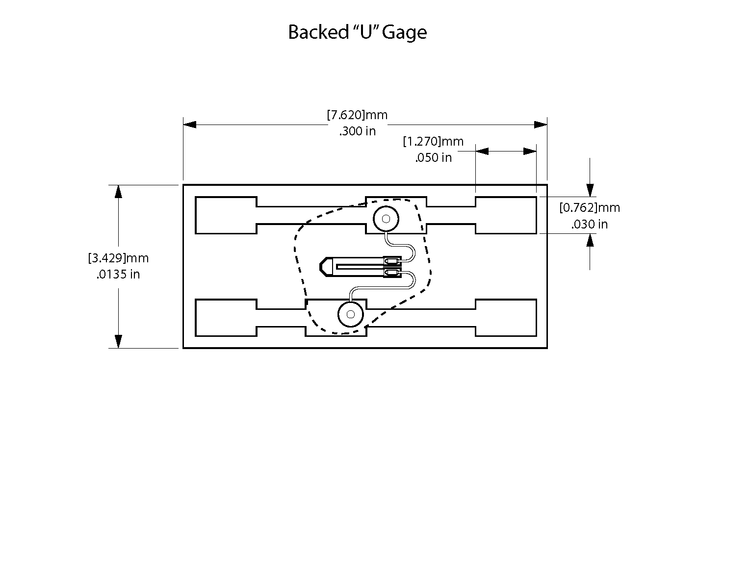
Gage Design
"Bar Shaped Gage - Lead Wires exit the ends of each side of gage

“U” Shaped Gage - Lead Wires Exit the same side of gage. These gages are also useful since the length is less and for the same length and resistivity, we can offer twice the resistance.

“M” Shaped Gage - Lead Wires Exit the same side of gage.

Gages are available between 10 ohms and 10,000 ohms.
Special gages are available for up to 800°F operation.
| Piezo-Metrics: PCB, Single Backed U-Gage | |
| UNLESS OTHERWISE SPECIFIED Dimensions are in inches tolerances: Angular: mach ±0*30 One place decimal ±0.03 Two place decimal ±0.010 Three place Decimal ± .005 All dia .005 Tir. Radii .005 Max Surface finish |
Drawn: 10/08/13 |
| PROPRIETARY AND CONFIDENTIAL The information contained in this drawing is the sole property of Piezo-Metrics. Reproduction in part or as a whole without the written permission of Piezo-Metrics is prohibited. | Checked: 10/08/13 |
| Piezo-Metrics: PCB, Single Backed Gage (Gages) | |
| UNLESS OTHERWISE SPECIFIED Dimensions are in inches tolerances: Angular: mach ±0*30 One place decimal ±0.03 Two place decimal ±0.010 Three place Decimal ± .005 All dia .005 Tir. Radii .005 Max Surface finish |
Drawn: 08/14/13 |
| PROPRIETARY AND CONFIDENTIAL The information contained in this drawing is the sole property of Piezo-Metrics. Reproduction in part or as a whole without the written permission of Piezo-Metrics is prohibited. | Checked: 08/14/13 |
| Piezo-Metrics: PCB, Single Backed Gage | |
| UNLESS OTHERWISE SPECIFIED Dimensions are in inches tolerances: Angular: mach ±0*30 One place decimal ±0.03 Two place decimal ±0.010 Three place Decimal ± .005 All dia .005 Tir. Radii .005 Max Surface finish |
Drawn: 08/14/13 |
| PROPRIETARY AND CONFIDENTIAL The information contained in this drawing is the sole property of Piezo-Metrics. Reproduction in part or as a whole without the written permission of Piezo-Metrics is prohibited. | Checked: 08/14/13 |
